
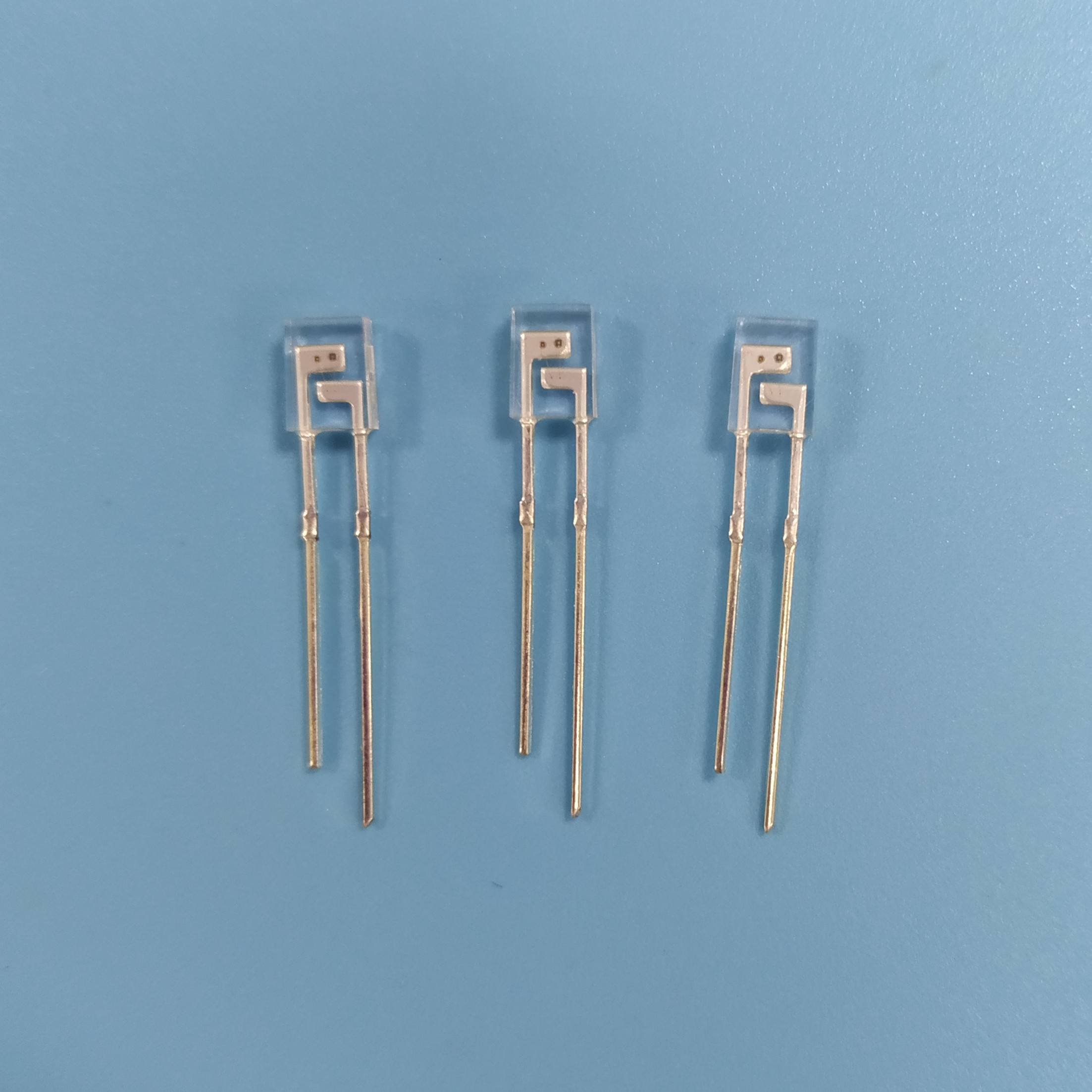
Why the Wavelength Pair Is Not a Free Choice
Pulse oximetry works by comparing how much light is absorbed at two wavelengths as blood pulses through tissue. Oxygenated and deoxygenated haemoglobin absorb differently, and the way that difference changes between the two wavelengths is what allows oxygen saturation to be calculated.
Jiangmen City Yiyang Infrared Semi-conductor Co., Ltd (Yiyang Optoelectronics YY) develops and packages infrared emitting and receiving components for medical monitoring applications in Jiangmen, Guangdong, producing dual-wavelength emitters and photodiode receivers designed as matching pairs for pulse oximeter probes.
The wavelength combination is therefore a metrological decision, not a design preference:
| Channel | Wavelength | Role in the measurement |
|---|---|---|
| Red | 660nm | Absorption is strongly dependent on oxygen saturation |
| Near-infrared | 905nm | Absorption is comparatively insensitive to saturation, providing the reference |
Two consequences follow. The pair must stay paired. Changing one wavelength without re-deriving the calibration invalidates the measurement, so a probe built with a 660nm/940nm combination is not a drop-in substitute for a 660nm/905nm design. Batch consistency matters more than absolute performance. Because saturation is computed from a ratio, small shifts in either wavelength create a proportional error in the result; a supplier whose emitters drift between batches produces probes that need recalibrating between batches.
The Emitter: Two Chips, One Package
A dual-wavelength SpO₂ emitter integrates both chips in a single body rather than combining two separate lamps on the board. Two package families are standard.
| Package | Structure | Typical application |
|---|---|---|
| DIP dual-wavelength emitter | Square flat-top through-hole body; 660nm red chip and 905nm near-infrared chip; two-lead structure | Pulse oximeter probes, fingertip oximeters, wearable SpO₂ modules |
| SMD dual-wavelength LED | 2-pin surface-mount body; 660nm and 905nm chips in one package; gold-plated pads | Compact and disposable probes, thin wearable modules, automated SMT production |
Integrating both chips in one package is not merely a convenience. It fixes the centre-to-centre distance and orientation of the two emitting chips at the factory, which is what makes the two channels illuminate the same tissue volume through the same optical path. In a discrete two-lamp design that geometry is set by the customer's placement accuracy and can vary between units; in an integrated package it is a controlled property of the part.
The SMD variant adds a further benefit for high-volume probe production: a 2-pin surface-mount device can be placed by the same automated line as the photodiode, so the entire optical pair is positioned by one machine with one set of fiducials.
The Receiver: Matched to the Pair, Not Chosen Independently
The photodiode in a SpO₂ design is specified against the emitter pair, and four figures define the match.
| Parameter | Target for SpO₂ | Reason |
|---|---|---|
| Spectral response range | 400–1100nm, covering both 660nm and 905nm | Both channels must be detected with the same device |
| Photosensitive area | Large square area | Collects the diffuse transmitted light; the signal is small |
| Dark current | Ultra-low | Sets the noise floor for a small modulating signal |
| Photoelectric linearity | Wide linear range | The ratio calculation assumes a linear response |
| Reverse voltage | ≥ 30 V capability | Allows the bias to be chosen for noise versus speed |
Linear response is the requirement most often overlooked. The saturation calculation is a ratio of ratios, and it presumes that photocurrent is proportional to received optical power across the whole working range. A receiver that compresses at high light levels, or drifts at low ones, distorts the ratio — and the resulting error is systematic, not random, so it does not average out across measurements.
Packages used for the receiver side follow the probe type: square DIP photodiode receivers with a large photosensitive window and gold-plated leads for reusable probes, and miniature square SMD receivers with heightened gold-plated pads for disposable probes and slim wearable modules, where PCB space is at a premium.
Optical Geometry and the Design of the Probe
The emitter and receiver must be positioned so that the light path passes through the tissue volume of interest, and the geometry is constrained by physics rather than by preference.
- Separation distance. Too close, and light reaches the detector without passing through pulsatile tissue, reducing the modulation depth the algorithm depends on. Too far, and the signal falls below the noise floor of the receiver.
- Alignment and shielding. Direct optical coupling between emitter and receiver — light that bypasses the tissue entirely — adds a constant baseline that carries no saturation information and reduces the usable modulation. Probe design uses opaque barriers between the two.
- Ambient light rejection. A filtered black epoxy receiver body blocks indoor and outdoor visible light, which is why the black filtered receiver is the standard choice rather than a clear one.
Supplying the emitter and receiver as a matched pair from one manufacturer is the practical way to control this: the emitting chips are in a known relationship to each other, the receiver's window is a known area, and the customer's placement work is reduced to a single alignment task.
SMT Process Rules That Decide Probe Yield
For surface-mount SpO₂ assemblies, the process specification is part of the component specification. Four rules determine whether a production run yields working probes.
- Reflow peak temperature control. A recommended peak of ≤260 °C with high-temperature exposure within about 10 seconds. Exceeding this damages the chip and produces a probe that passes a visual inspection and fails photometrically.
- Polarity identification before placement. Markings on the back face identify anode and cathode. A reverse-connected emitter or receiver does not work, and the fault is invisible after reflow.
- Optical path alignment. The receiver must be positioned so that the emitter's illuminated area fully covers the photosensitive window. Partial coverage reduces the effective area and therefore the signal, and it is a placement problem rather than a component problem.
- Moisture-proof handling. Surface-mount parts are supplied in vacuum moisture-proof tape. Mounting within 24 hours of opening is recommended; longer storage should remain sealed and moisture-proof. Absorbed moisture causes delamination and cracking during reflow — a failure that appears after the assembly, not before it.
Two further manufacturing controls are worth stating for medical-grade production. Dust-free packaging conditions prevent particulate contamination of the optical surfaces, which scatters light and reduces signal. Full inspection of photocurrent, dark current and spectral response on each batch is what converts a material specification into a deliverable consistency guarantee, and it is the reason medical customers ask for the test data rather than only a certificate.
SpO₂ Optical Pair Specification Checklist
- Wavelength pair stated as 660nm and 905nm, with the bin tolerance on each channel.
- Binning consistency requirement stated, since the ratio calculation converts wavelength drift into measurement error.
- Emitter package chosen for the probe type — DIP for reusable probes, SMD for disposable and compact designs.
- Receiver spectral range confirmed to cover both channels — 400–1100nm — with a black filtered body for ambient rejection.
- Dark current specified as ultra-low with its bias and temperature condition.
- Linear response range stated, because the ratio algorithm assumes it.
- Photosensitive area stated and matched to the illuminated area at the working geometry.
- Emitter and receiver sourced as a matched pair to fix the optical centre distance.
- SMT limits specified — reflow peak ≤260 °C, exposure ≤10 s, polarity marking, and the 24-hour mounting window from vacuum tape.
- Batch test data agreed for photocurrent, dark current and spectral response, plus RoHS and lead-free compliance for export.
Optical Pairs That Keep Their Calibration
In pulse oximetry the component choice is inseparable from the measurement: the wavelength pair is fixed by the physics, the package fixes the geometry, and the process fixes the yield. Specifying the emitter and receiver together, with the bin tolerance and the process limits stated, is what makes a probe that measures the same on the first unit and the thousandth.
Send us your probe type, target geometry and volume, and we will return a matched emitter and receiver specification with the wavelength bins, package options, dark current and linearity data, and the SMT handling requirements confirmed — together with pair samples for photometric evaluation.