
The Receiver Is Half the Optical System
Infrared designs are usually discussed in terms of the emitter — its wavelength, its power, its angle. The receiver is specified later, often by matching a wavelength, and it is the receiver that decides whether the system works in the real optical conditions: ambient light, distance, alignment tolerance and required speed.
Jiangmen City Yiyang Infrared Semi-conductor Co., Ltd (Yiyang Optoelectronics YY) packages infrared photodiode receivers, emitting diodes and receiver modules in Jiangmen, Guangdong, supplying medical monitoring, security alarm, smart home and industrial sensing applications for over 13 years. The specification conversations that determine whether a receiver performs are about four figures, and they interact.
1. Spectral Response Range: Does It See Your Emitter
The spectral range is the band over which the detector converts light into current. For silicon photodiodes this is broadly 400–1100nm, but the usable band depends on the package.
| Parameter | Typical value | What it decides |
|---|---|---|
| Spectral response range (package-dependent) | 400–1100nm, or 600–1100nm with black filtering | Whether the emitter's wavelength falls inside the usable band |
| Receiver band for 940nm remote-control use | 840–1100nm | Black epoxy filters visible light while passing the 940nm signal |
| Peak sensitivity wavelength | Approximately 850–950nm | Highest conversion efficiency region for silicon |
The subtlety is that the package changes the effective range. A clear epoxy photodiode responds across the full silicon band, including visible light — which in a remote-control or beam-break application is exactly the noise you do not want. A black filtered epoxy body blocks most visible ambient light and passes the infrared band, shifting the usable range to roughly 840–1100nm. Two parts with the same chip and different epoxy are therefore different products.
The specification should state the filtered range, not the chip's raw range, whenever the application involves ambient light. For indoor remote control and security beam detection, the filtered part is almost always the correct choice.
2. Responsivity: Current per Watt of Light
Responsivity is the photocurrent produced per unit of incident optical power, expressed in amperes per watt (A/W). It is the figure that converts an optical design into an electrical signal.
| Wavelength | Typical silicon responsivity | Implication |
|---|---|---|
| 660nm | ≈ 0.4 A/W | Visible red; used in oximetry as the reference channel |
| 850nm | ≈ 0.6 A/W | High efficiency; common for sensing and imaging |
| 905nm | ≈ 0.6 A/W | Near-infrared oximetry channel and range-finding |
| 940nm | ≈ 0.5–0.6 A/W | Still efficient, and invisible — the remote-control standard |
| 1050nm and beyond | Falls steeply | Approaching the silicon band edge; low output, high temperature sensitivity |
Three design consequences follow. Responsivity depends on wavelength, so a receiver specified for 940nm performs measurably less well at 1050nm even though both are "infrared". Responsivity is temperature dependent: it rises slightly with temperature for silicon while dark current rises much faster, so the signal-to-noise ratio usually gets worse even though the absolute signal does not. The quoted figure is a room-temperature value; any design that must work across −20 °C to +85 °C should have the responsivity and dark current considered at both ends of the range.
3. Dark Current: The Noise Floor
Dark current is the current that flows with no light at all. It is the single most important figure for any application measuring a small optical signal.
| Factor | Effect on dark current |
|---|---|
| Temperature | Roughly doubles for every 10 °C rise — the dominant influence |
| Reverse voltage | Increases with bias; a photodiode at 0 V has far lower dark current than at 30 V |
| Chip area | Proportional to photosensitive area — the trade-off against signal |
| Material and process quality | Well-controlled processing and passivation materially reduce it |
Two specification points are routinely missed. The bias condition must be stated. A dark current quoted at 0 V (photovoltaic mode) and one quoted at 5 V reverse (photoconductive mode) can differ by orders of magnitude; a figure without its bias is not comparable. Dark current sets the practical signal floor, not the sensitivity ceiling. A receiver with excellent responsivity but high dark current cannot resolve a small signal in a dark measurement, which is precisely the condition in transmission oximetry through a finger or in a dark optical path.
For applications requiring the lowest noise — pulse oximetry, precision optical sensing, low-level light detection — the correct specification is an ultra-low dark current requirement combined with a defined bias and temperature, and the supplier should be asked to confirm the test condition rather than only the typical value.
4. Reverse Voltage, Capacitance and Response Time
These three determine how fast the receiver can work, and they form a single trade-off.
| Parameter | Typical value | Trade-off |
|---|---|---|
| Reverse voltage Vr (max) | ≥ 30 V for many silicon PD receivers | More bias reduces capacitance and speeds response, but raises dark current |
| Junction capacitance | Decreases as reverse bias increases | Lower capacitance gives faster response and wider bandwidth |
| Response time (rise/fall) | Nanoseconds to microseconds depending on area and bias | Faster response generally requires a smaller active area |
| Photosensitive area | Larger area collects more light | Larger area raises capacitance and dark current, slowing response |
The engineering summary is that there is no universally better photodiode, only a better match. A large-area device with low bias gives maximum signal and lowest dark current but is slow; a small-area device at high bias is fast but collects less light and has more dark current.
For a pulse oximeter, the signal is a small modulating component on a large background, and the modulation frequency is low — tens of hertz to a few kilohertz. That application therefore wants a large photosensitive area and low dark current, and does not need nanosecond speed. For a beam-break sensor interrupting a light path at high repetition rates, the priorities invert. Stating the required bandwidth alongside the signal level lets the supplier choose the right device instead of the fastest one.
5. Package, Filtering and Mounting
| Package | Character | Typical use |
|---|---|---|
| 5mm round black filtered DIP | Filters visible light, extended leads trimmable | Remote control, sensing, security, industrial automation |
| Square DIP PD receiver | Square light window, large photosensitive chip, gold-plated leads | Pulse oximeters, optical detection equipment |
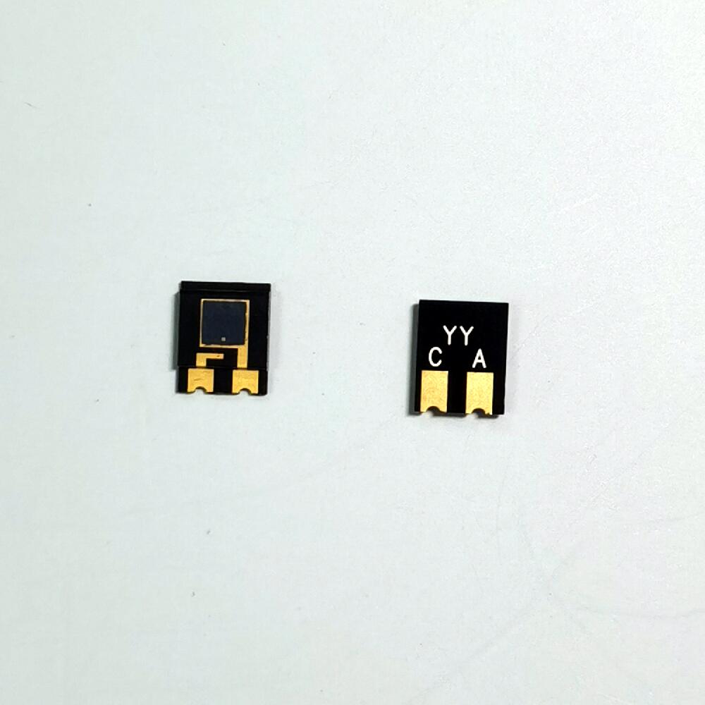
| Miniature square SMD PD receiver | Low profile, gold-plated pads, reflow compatible | Disposable SpO₂ probes, wristband modules, slim fingertip oximeters |
| Bridge-type receiver head | Bridge lens structure, black filtering | Receiver heads for compact appliances and sensing products |
For SMD receivers, three process rules belong in the specification rather than in a separate handling note. Reflow peak temperature is typically limited to ≤260 °C with high-temperature exposure within about 10 seconds, because exceeding it damages the chip. Polarity marking must be identified on the part — anode and cathode markings on the back face — since reverse connection is not permitted and a mis-oriented part fails silently. Moisture-proof packaging is part of the product: SMD receivers are supplied in vacuum moisture-proof tape, and mounting within 24 hours of opening is recommended, with long-term storage kept sealed.
Photodiode Receiver Specification Checklist
- Filtered spectral range stated (e.g. 840–1100nm), not the raw chip range, where ambient light is present.
- Responsivity stated at the system wavelength, not at the peak, and with its temperature condition.
- Dark current stated with its bias and temperature — a figure without these is not comparable.
- Photosensitive area stated, since it drives signal, capacitance and dark current together.
- Maximum reverse voltage stated and the intended operating bias agreed.
- Response time or bandwidth stated against the modulation frequency the system actually uses.
- Temperature range stated for the fully assembled device, covering the real operating environment.
- Package and filtering identified by part number, since epoxy colour changes the product.
- SMD process limits stated — reflow peak, polarity marking and moisture-proof packaging with the 24-hour mounting window.
- Environmental compliance confirmed — RoHS and lead-free with report reference, which matters for medical and export applications.
Receivers That Work in the Real Optical Environment
Photodiode selection is a set of deliberate trade-offs between signal, noise and speed. A specification that states only a wavelength leaves every one of those trade-offs to be discovered during testing, in the conditions least convenient for changing a design.
Send us your emitter wavelength, expected signal level and required bandwidth, and we will return a receiver specification with the filtered range, responsivity, dark current at the agreed bias, active area and package stated for each candidate, with samples for measurement in your own optical setup.