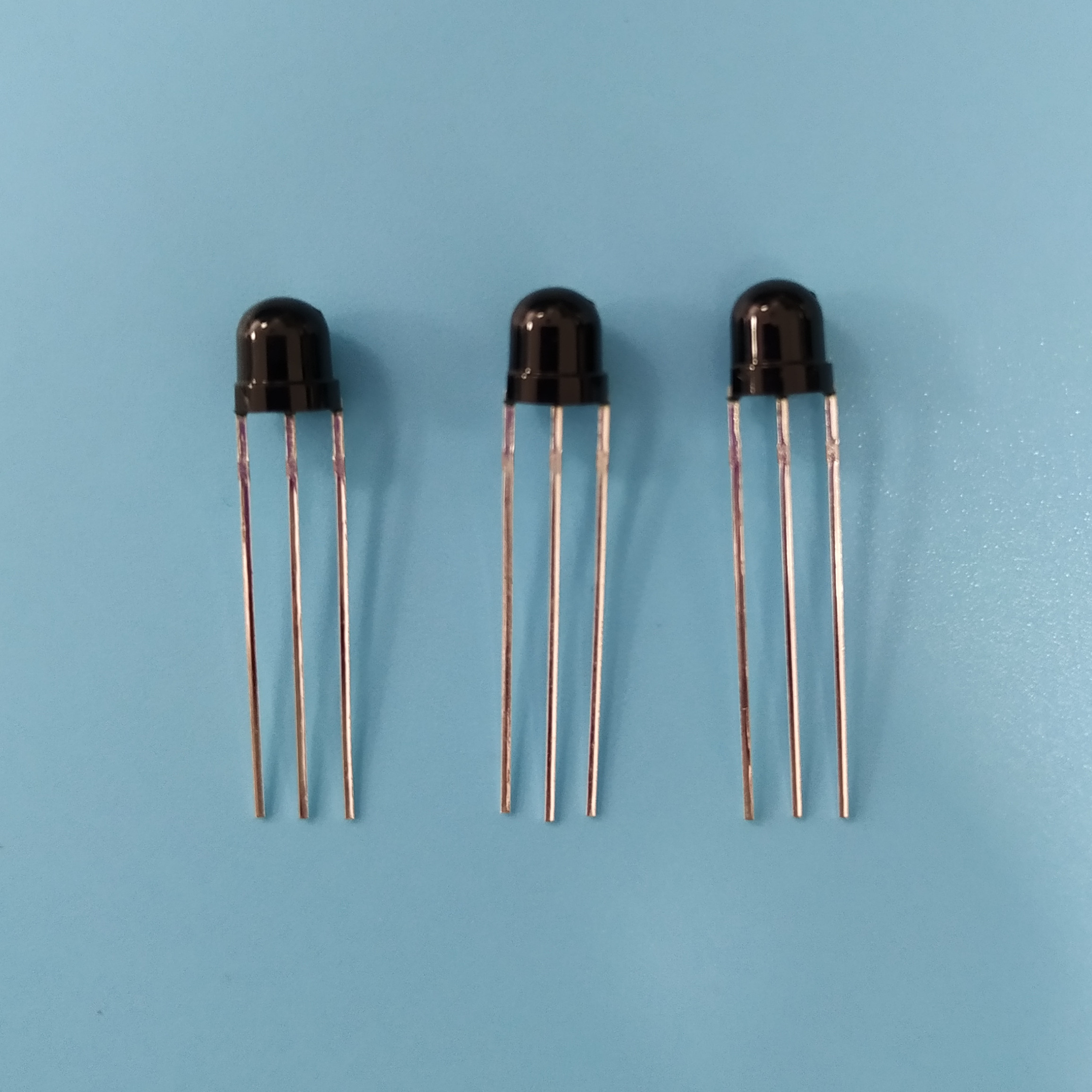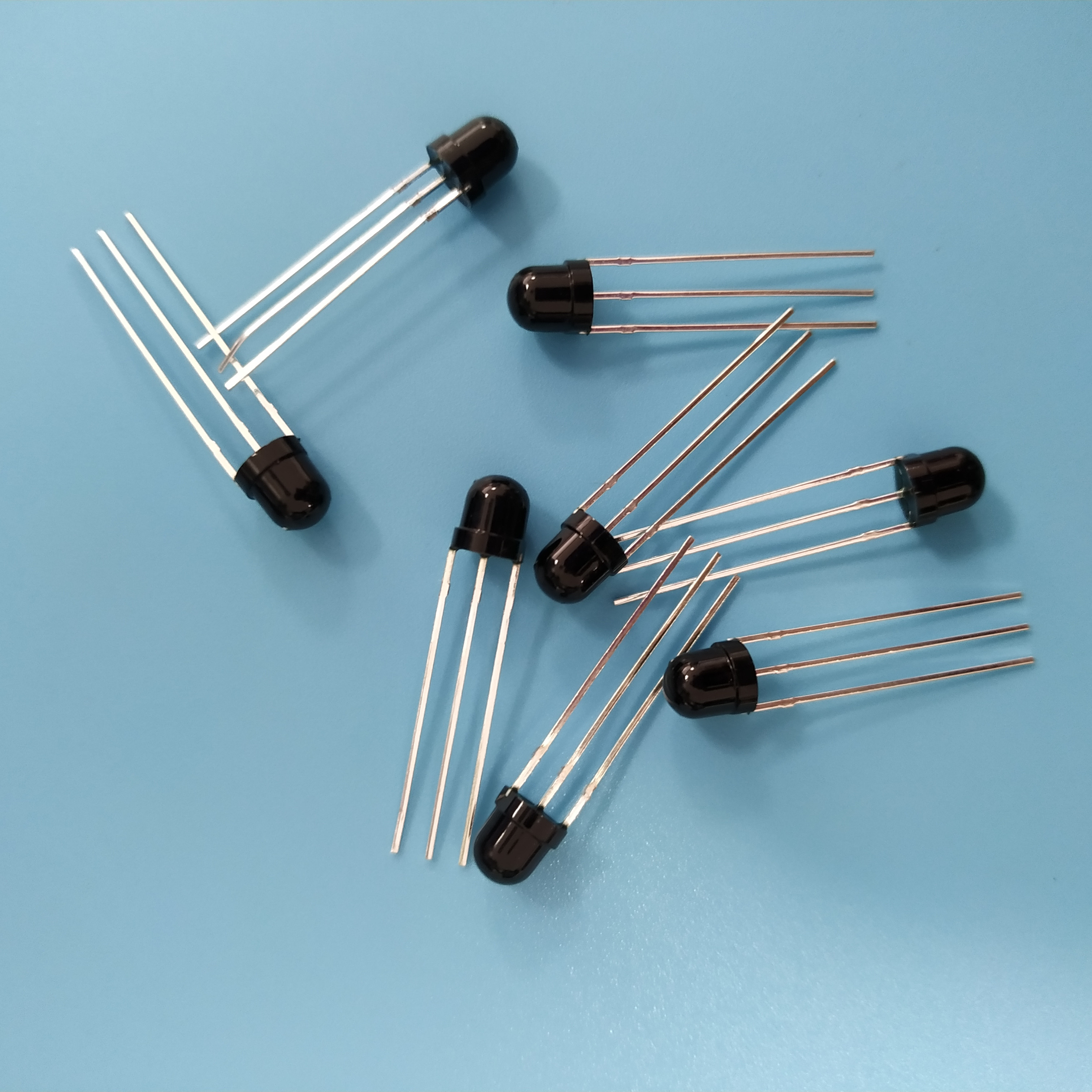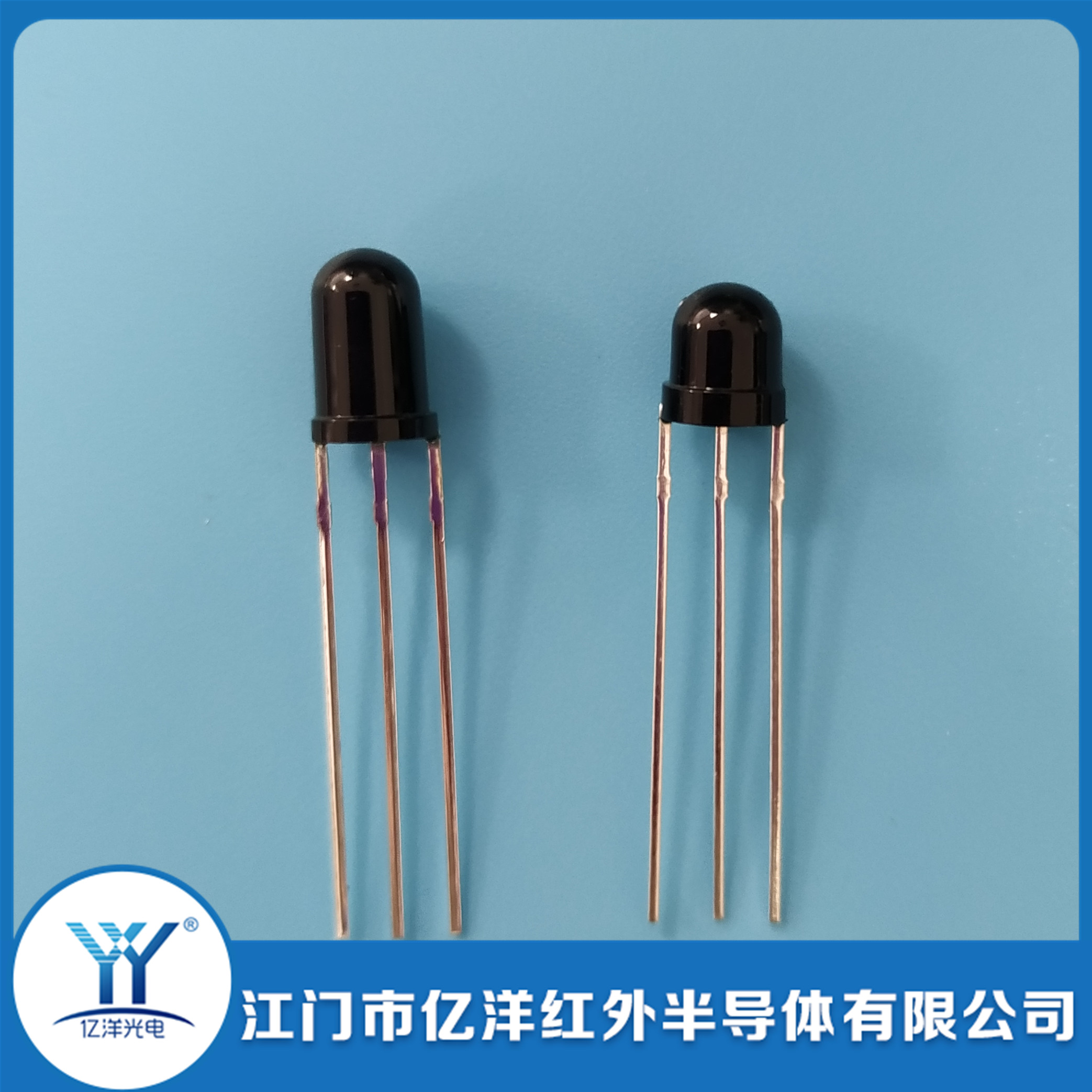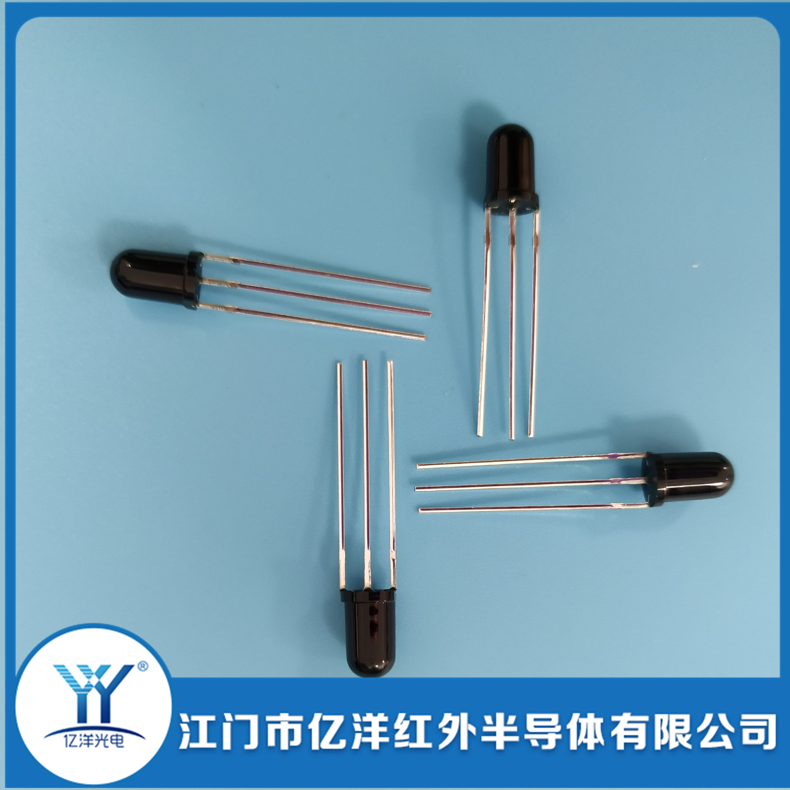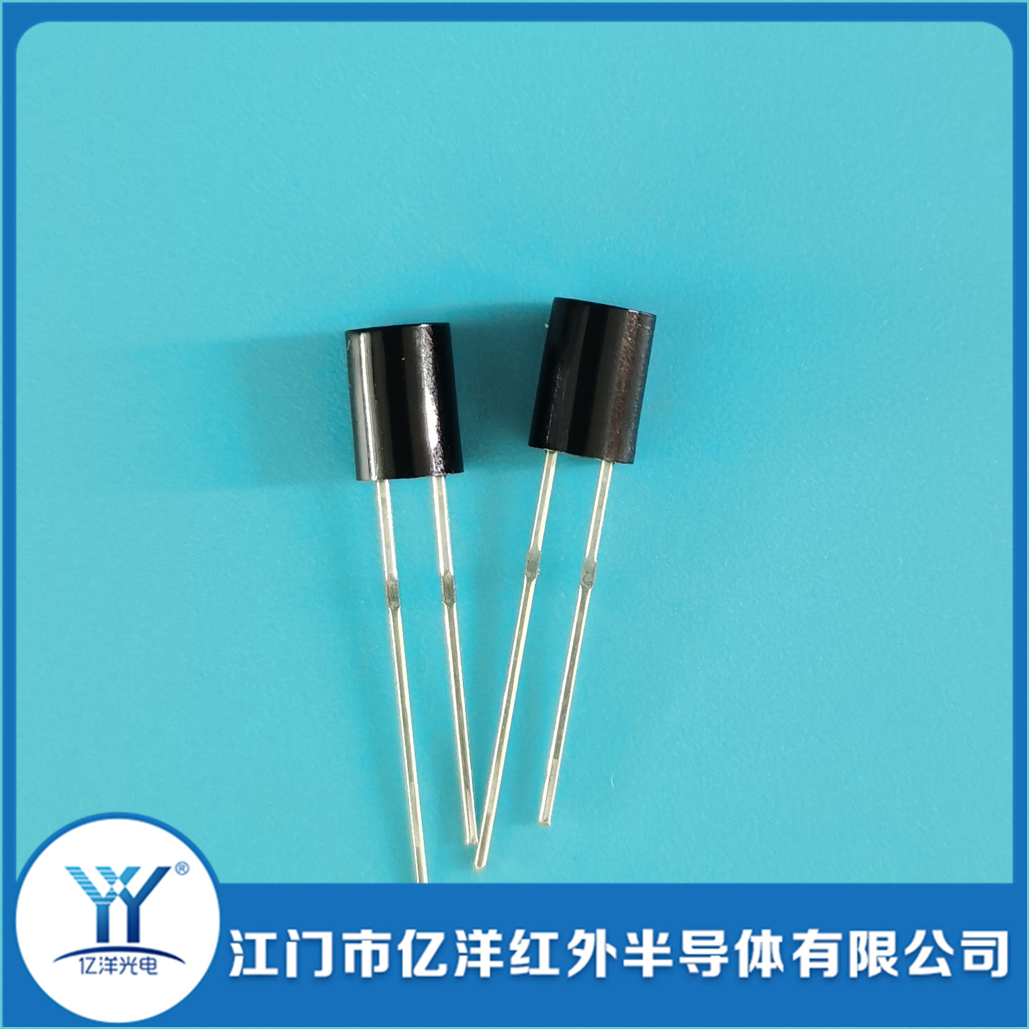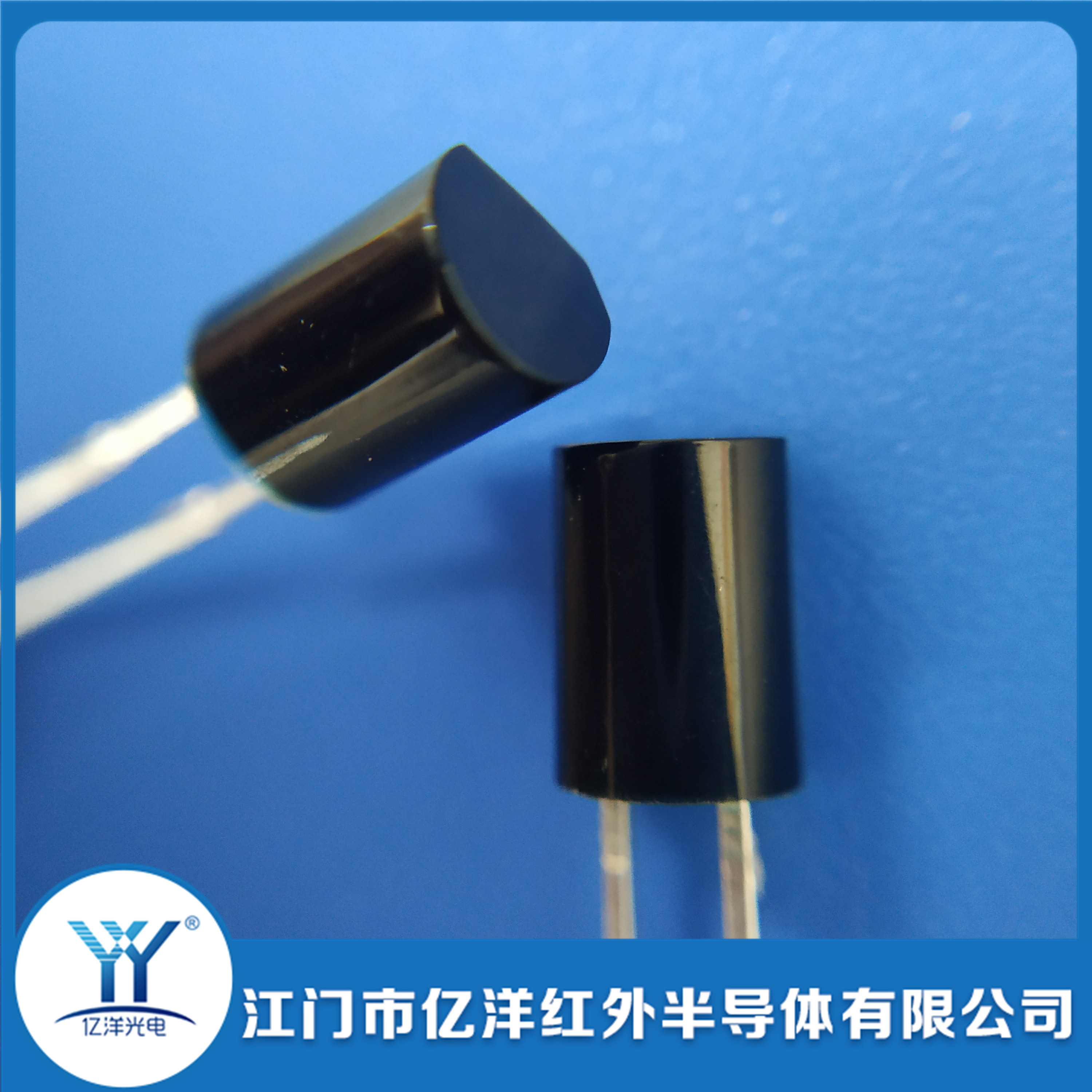
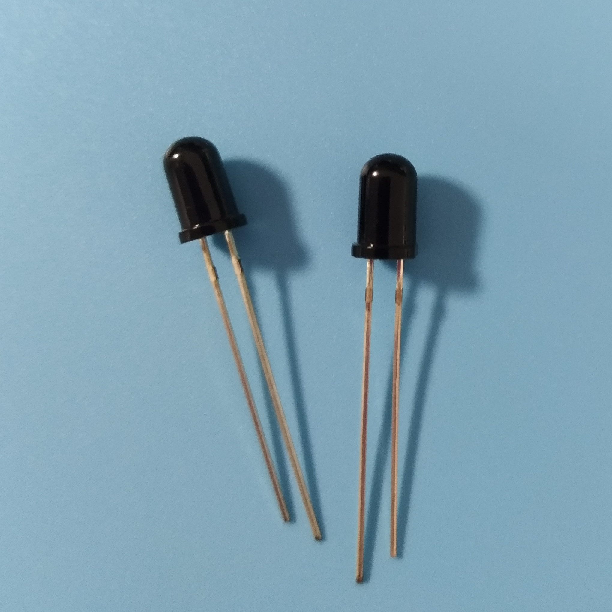
A purchase order for an infrared emitter or photodiode usually arrives as a discussion about optics. The wavelength, the radiant intensity, the sensitivity — those are the numbers that get argued over in the specification meeting. Then the samples come back and the part does not fit the board, or the insertion head cannot grip it, or the bend collides with the housing. At that point the order turns into a lead and package problem, and the whole schedule moves.
Jiangmen City Yiyang Infrared Semi-conductor Co., Ltd, operating as Yiyang Optoelectronics YY, has packaged infrared emitting diodes, photodiode receivers and remote-control receiver heads in Jiangmen, Guangdong for more than 13 years, at a daily capacity of 600K pieces, with exports to over 40 countries. The customization requests that arrive most often are not exotic optical specifications. They are lead length, lead form, lead pitch and epoxy colour — four items that decide whether a correctly specified device can be assembled at all.
This article covers what can be changed on the lead frame and the package body, which figures need to be stated on a drawing, and where the boundary sits between modifying a standard part and opening a mold.
Why the Lead Is Part of the Optical Design
An infrared component sits at a fixed distance from its counterpart. In a beam-break sensor, a reflective switch or a pulse oximeter probe, the emitter and the receiver must be held at a defined separation and a defined angle to each other. That geometry is set by the PCB pads the leads land on and by the height the package stands above the board. Change the lead length and the optical centre height changes. Change the pitch and the pair separation changes.
So a lead customization is rarely cosmetic. Three cases account for most of them:
| Reason for customization | What actually drives it | Typical fix |
|---|---|---|
| Board does not match the standard footprint | Existing PCB layout, pad pitch inherited from an older design | Custom pitch, or bent leads to reach offset pads |
| Component must clear a housing or gasket | Mechanical envelope, lens or light-pipe position, potting depth | Shortened leads, or a bent form that routes around the obstruction |
| Assembly line cannot handle the standard form | Insertion head jaw travel, feeder height, wave-solder pallet | Equal-length or long/short leads, straight versus pre-bent, tape or bag packaging |
In all three, the lead is doing two jobs at once: making electrical contact, and setting the mechanical position of an optical element. That is why the drawing has to describe it precisely. "Standard leads" is not a description when the assembly depends on the figure. It is worth settling the optical figures first — how an emitter is specified and how a receiver is specified both treat the lead form as part of the order line rather than an afterthought.
1. Lead Length: Long, Short and Equal Length
Through-hole infrared parts are offered with several lead length conventions, and each one carries a different assumption about how polarity will be identified at assembly.
| Lead form | Geometry | Polarity identification | Where it is used |
|---|---|---|---|
| Long / short (unequal) | Anode lead longer than cathode lead | By length difference — the long lead is the anode | Manual and semi-automatic insertion; the classic convention |
| Equal length | Both leads the same length | Requires a body marking, flat on the epoxy, or a notch | Automatic insertion where the head grips both leads at once |
| Extended / untrimmed | Deliberately over-length, e.g. 24mm and above | Same as the base form | Double-sided boards, deep housings, wiring runs; trimmed on site |
| Pre-trimmed to final length | Cut at the factory to a stated figure | As specified | Volume production where trimming is done by machine anyway |
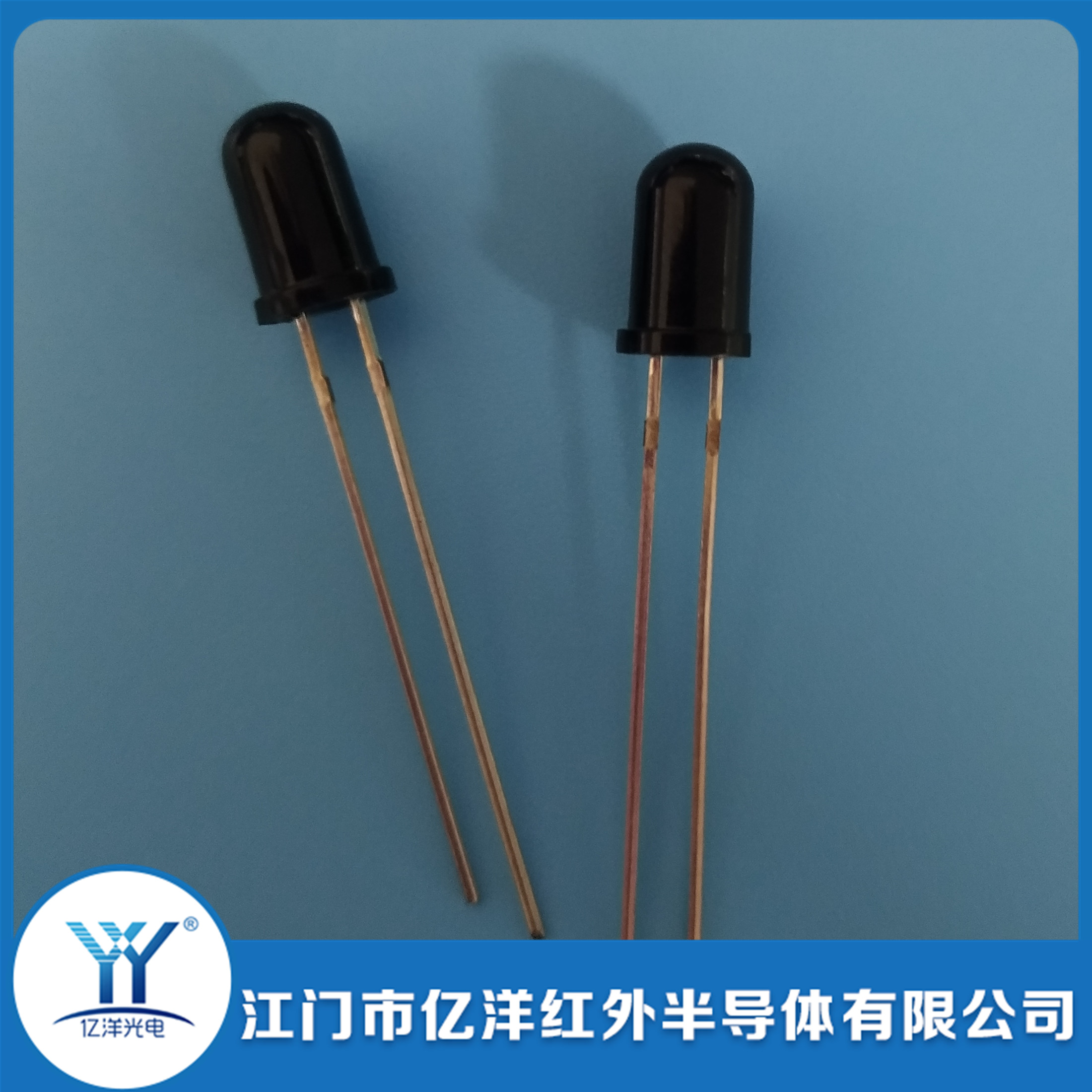
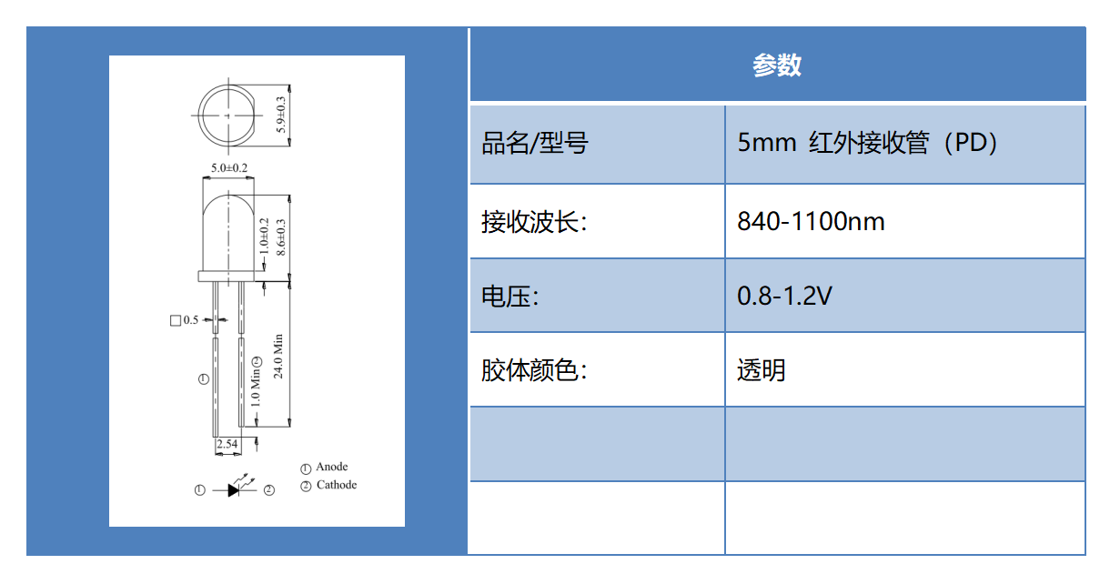
The extended-lead approach deserves attention because it removes a sourcing decision rather than adding one. A 5mm receiver photodiode supplied with leads of 24mm or more total length can be trimmed to whatever the pad spacing and board stack-up require, without a tooling change and without a second part number. For a design that is still moving — a probe housing under revision, a fixture built per installation — a single long-lead part covers the range. The cut is made with side cutters or a trimming die, and the exposed cross-section must be re-tinned if the assembly will sit before soldering.
There is a real trade-off in pre-trimming. A factory cut is square, burr-controlled and consistent across the batch; a hand cut is none of those things, and a burr on a plated lead is where a cold solder joint starts. If the assembly volume justifies it, pre-trimmed leads at a stated length are more reliable than site trimming.
2. Lead Pitch: 1.27mm, 2.0mm and 2.54mm
Pitch is the centre-to-centre distance between adjacent leads, and for infrared through-hole parts the standard options are 1.27mm, 2.0mm and 2.54mm. The 2.54mm figure dominates because it matches the long-established 0.1 inch prototyping and breadboard grid; the tighter pitches exist because a smaller package body or a smaller optical pair separation demands them.
Pitch interacts with three things that are easy to overlook:
- Pad geometry on the board. A 2.54mm pitch part will not enter a 2.0mm hole pattern without bending, and a forced bend at the lead root is where epoxy cracking begins.
- Solder bridging. The tighter the pitch, the closer the meniscus of two adjacent joints. Wave-soldered boards at 1.27mm pitch need a solder mask dam between pads and a correctly sized pallet cut-out.
- Optical separation. For an emitter–receiver pair on the same board, pitch sets the baseline between the two optical axes, which sets the triangulation or transmission geometry.
Standard pitch covers the majority of designs. When it does not, there are two routes: bend the leads to reach a non-standard pad spacing, or open a mold for a package with a different lead frame. Bending is fast and cheap but consumes board height and introduces a stress point. A new mold is the correct answer only when the pitch is fixed by the product — typically when the same package will be used across a family of boards for several years. Yiyang Infrared supports mold opening for special lead spacing, and the decision point is usually the annual volume against the tooling cost.
3. Bent Leads: Angle, Root Radius and Stress
A bent lead form solves a mechanical problem: the optical axis needs to point somewhere the straight lead cannot reach, or the package must lie flat while the board sits at an angle. Bending is a forming operation on a plated copper lead, and the details of that operation decide long-term reliability.
| Parameter | Why it matters | What to state on the drawing |
|---|---|---|
| Bend angle | Sets the optical axis direction; small errors become large errors at a distance | Angle in degrees, with tolerance |
| Bend position | Distance from the epoxy body to the start of the bend — too close and the epoxy is stressed | Dimension from the package seating plane |
| Root radius | A sharp internal radius concentrates stress and can crack the plating; a generous radius distributes it | Minimum radius, or "no sharp bends" as a note |
| Co-planarity of the lead ends | Both ends must sit flat on the pads for a sound joint; a twisted form lifts one | Flatness tolerance across the two lead ends |
| Insertion clearance | Bent forms are usually hand- or selectively placed, not fed through a standard inserter | Assembly method, so packaging is chosen to match |
Two failure modes recur with bent leads. The first is plating cracking at the bend: the nickel or silver plating on a copper lead is ductile enough for a single generous bend but not for a sharp fold, and a crack there is invisible until it oxidizes and the joint goes intermittent months later. The second is epoxy-to-lead separation at the package exit, which happens when the lead is bent close to the body and the bending force is transferred into the encapsulation. Both are avoided by specifying the bend position and radius rather than only the final angle.
The structural form matters as well. An L-shaped bend puts the lead along the board; a Z-shaped offset moves the lead laterally while keeping the package upright; a J-form curls the lead for a spring contact. Each has a different footprint and a different assembly sequence. A drawing that shows only "bent lead" is ambiguous between all three.
4. Cut Leads and the Question of Solderability
Cutting a lead creates a fresh metal surface. On a plated lead, the cut exposes the copper core, and that core oxidizes. The consequence is not immediate — the part still looks correct — but a cut end that has sat in humid air for weeks will wet poorly, and in a wave-solder process the cut end is exactly the surface that must draw solder up the barrel.
Practical rules follow from this. Cut leads should be trimmed close to the assembly date, not months before it. Storage between cutting and soldering should be dry and sealed. Where a long interval is unavoidable, a factory pre-trim with a controlled cut and immediate re-packaging is more dependable than a site cut followed by open storage. For silver-plated and gold-plated leads the concern is the same in kind and larger in degree, because the plating is what provides the low-resistance, oxidation-resistant surface in the first place.
5. Epoxy Colour: Transparent, Blue-Transmitting and Black Filtered
The epoxy body is a lens, a mechanical housing and an optical filter at the same time. Its colour is therefore not a cosmetic variable, and the three common options behave differently.
| Epoxy type | Optical function | Used on | Notes |
|---|---|---|---|
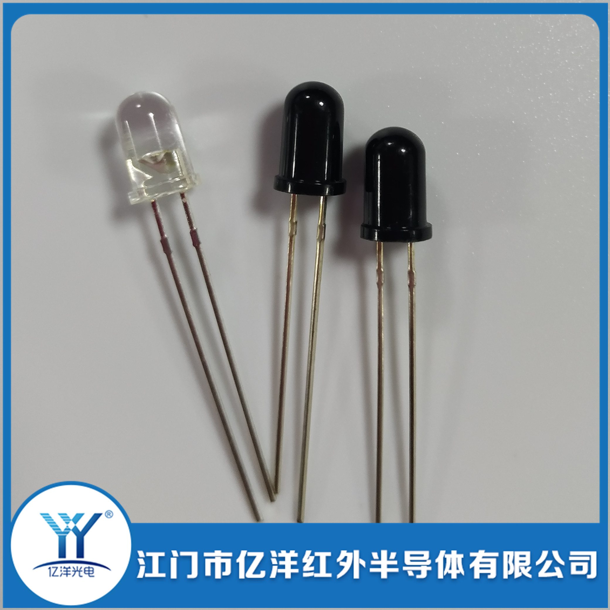
| Water clear / transparent | Maximum transmission across the emitted or detected band | Emitters, general receivers | Highest output; no ambient light rejection |
| Blue infrared-transmitting | Passes infrared, suppresses part of the visible band | Emitters used where some visible rejection is wanted | Distinguishable by eye; useful for part identification on the line |
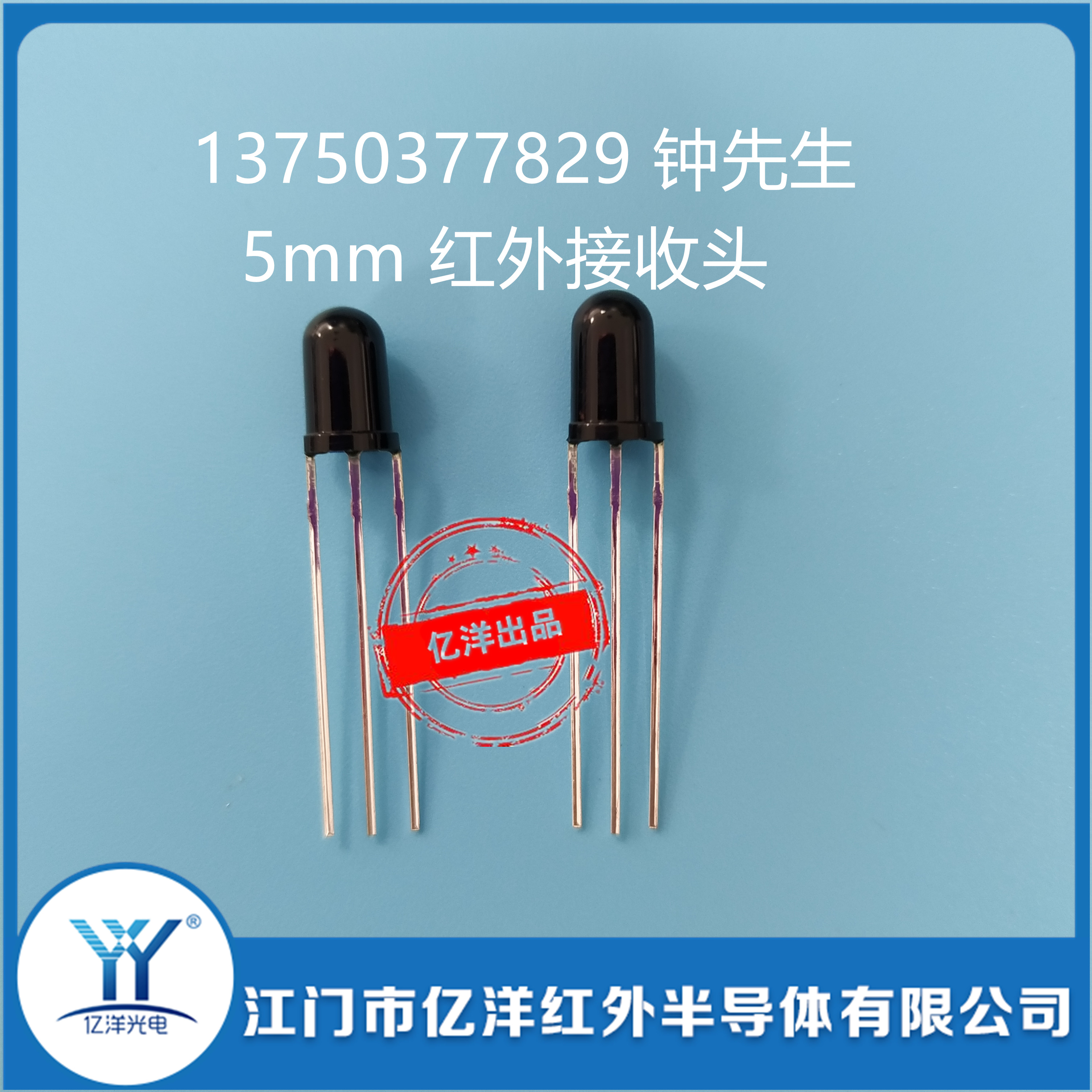
| Black filtered | Blocks visible and near-visible stray light; passes the infrared or red/near-infrared band | Photodiode receivers, receiver heads, pulse oximeter PDs | Essential under sunlight, LED lighting and white-light interference |
For a receiver, the black filtered body does substantive work. A photodiode with an unfiltered clear body responds to indoor LED lighting and daylight, and the resulting photocurrent appears as a baseline offset that the amplifier must reject. A black epoxy front end removes most of that at the source, which is why pulse oximeter receivers and remote-control receiver heads are black even though a clear body would deliver more signal. The trade is signal amplitude for ambient rejection, and for a receiver the trade is usually worth making.
Epoxy colour is also a mechanical variable. Black and clear bodies are not interchangeable at the part-number level even when the internal chip is identical, because the optical response differs. A substitution in production that is not reflected on the drawing will change the measured behaviour of the assembled unit.
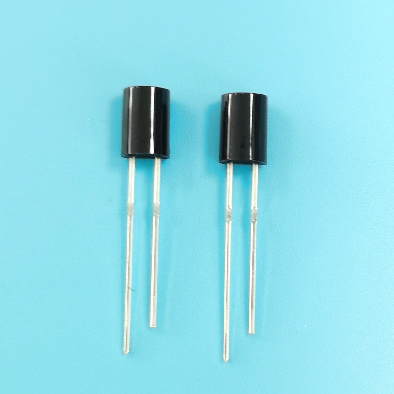
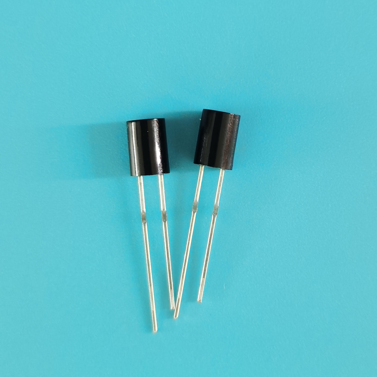
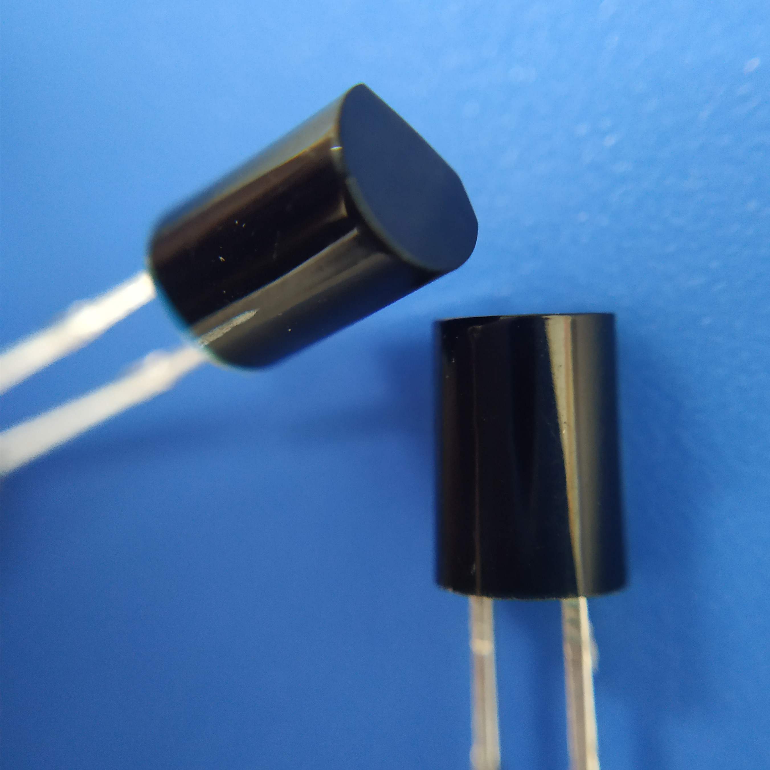
The lead form and the epoxy body interact more than the two tables above suggest. A bent lead changes the orientation of the package relative to the board, which changes the direction the epoxy lens faces — and that direction is the optical axis. A 5mm round receiver bent through 90° and a semi-circular receiving tube mounted straight are not optically equivalent even when the chips inside are the same. The drawing has to describe both halves of the geometry, not just the lead.
Customization Matrix: What Can Be Changed and What It Costs
| Item | Standard options | What it affects | When to raise it with the supplier |
|---|---|---|---|
| Lead length | Short, long, unequal, equal, extended (24mm and above) | Mounting height, optical centre, PCB stack-up | Whenever the board is not a direct match to the reference footprint |
| Lead pitch | 1.27mm / 2.0mm / 2.54mm; special spacing by mold opening | Pad fit, pair separation, solder bridging risk | When the board pitch is fixed and cannot be re-laid out |
| Lead form | Straight, L-bend, Z-bend, J-form; bent and cut | Optical axis direction, assembly method, footprint | When the optical axis cannot point straight down from the board |
| Epoxy colour | Clear, blue infrared-transmitting, black filtered | Transmission, ambient light rejection, part identification | When the unit will be used under sunlight, LED or white-light sources |
| Package size | 3mm, 5mm round, square, bridge-type head | Envelope, viewing geometry, board density | When the housing is designed around a specific envelope |
| Polarity marking | Lead length difference, flat, notch | Correct orientation at assembly | When leads are equal length or the insertion is automated |
Standard Part, Modification or New Mold
There are three routes from a requirement to a deliverable part, and choosing the wrong one costs either money or schedule.
- Standard part, as supplied. The fastest route. Validate the lead form, pitch and epoxy colour against the board before assuming a change is needed — the majority of requests are satisfied by a stocked configuration.
- Standard chip and package, customized lead frame or epoxy. Lead length, lead form, pitch within the existing tooling, and epoxy colour are all reachable without new tooling. Scheduling is measured in working days rather than weeks. This is where most genuine custom orders land.
- New mold. Justified when the package geometry itself must change: a special lead spacing outside the standard set, a body size that does not exist, a lens form the standard parts cannot provide. The cost is tooling, and the justification is a volume that will amortize it.
A useful test before opening a mold: can the requirement be met by bending an existing lead? A bent 2.54mm part reaching an offset pad solves a mechanical mismatch without tooling. A mold is the right answer when the pitch itself is wrong, not merely when the lead ends up in the wrong place. Once the lead is settled, the next question is usually how the part will be fed — see from drawing to reel for packaging and lead time — and, where the part is half of an emitter–receiver pair, matching the pair optically.
What to Put on the Drawing
A lead customization order fails in predictable places. A drawing that answers the following questions moves through sampling without a round trip:
- Package type and body dimensions — 3mm, 5mm round, square, bridge head, with the datum face identified.
- Lead length, measured from the seating plane — not from the top of the body, and with a tolerance.
- Polarity convention — which lead is the anode, and how it is identified if the leads are equal length.
- Lead pitch with tolerance, and whether the pitch is a fit requirement or an optical one.
- Lead form — straight, L, Z or J, with the bend position, angle and minimum root radius stated.
- Lead material and plating, if the standard tin or nickel-plated copper is not acceptable.
- Epoxy colour and its optical intent — clear, blue-transmitting or black-filtered, and the wavelength band to be passed.
- Assembly method — hand, semi-automatic insertion, automatic insertion, SMT — because it determines the packaging and the acceptable lead co-planarity.
- Target photoelectric parameters, so the lead change is not allowed to shift the optical behaviour.
- Annual quantity, which is what decides between lead modification and a new mold.
Two of these are routinely missing and cause most of the delay: the measurement datum for lead length, and the assembly method. A lead length quoted from the wrong face is a length the factory cannot hit, and an assembly method that is not stated leaves the packaging — bag or tape — to be guessed.
Leads Specified Before the Samples Ship
Lead length, lead pitch, lead form and epoxy colour are unglamorous variables, and that is why they are the ones that stop a build. They are also among the cheapest things to change — a different lead length or a bent form is a fixture change, not a new tool. The expensive version of the same request is discovering the mismatch after the probe housing has been tooled.
Yiyang Infrared supplies infrared emitters, photodiode receivers, receiver heads and emitter–receiver pairs with lead length, lead pitch, lead form and epoxy colour customized against a customer drawing, and with mold opening available where the package geometry has to change. Standard in-stock models ship in 1–3 days; customized models are typically scheduled within 3–7 days. Send the board footprint, the mechanical envelope and the assembly method, and the lead specification can be settled before the first sample is cut.
Before sending the drawing, it is worth checking the project against the rest of this series: the optical pair and SMT process rules for probe assemblies, and the supplier evaluation points that apply to any custom order. For background on the company and the range, see about Yiyang Infrared and the product knowledge archive.